The purpose of the parallel-in/ parallel-out shift register is to take in parallel data, shift it, then output it as shown below. A universal shift register is a do-everything device in addition to the parallel-in/ parallel-out function.


Above we apply four bit of data to a parallel-in/ parallel-out shift register at DA DB DC DD. The mode control, which may be multiple inputs, controls parallel loading vs shifting. The mode control may also control the direction of shifting in some real devices. The data will be shifted one bit position for each clock pulse. The shifted data is available at the outputs QA QB QC QD . The "data in" and "data out" are provided for cascading of multiple stages. Though, above, we can only cascade data for right shifting. We could accommodate cascading of left-shift data by adding a pair of left pointing signals, "data in" and "data out", above.
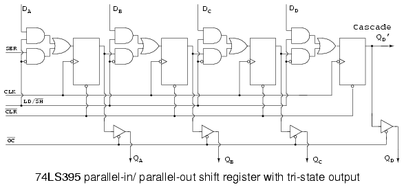
The internal details of a right shifting parallel-in/ parallel-out shift register are shown below. The tri-state buffers are not strictly necessary to the parallel-in/ parallel-out shift register, but are part of the real-world device shown below.
The 74LS395 so closely matches our concept of a hypothetical right shifting parallel-in/ parallel-out shift register that we use an overly simplified version of the data sheet details above. See the link to the full data sheet more more details, later in this chapter.
LD/SH' controls the AND-OR multiplexer at the data input to the FF's. If LD/SH'=1, the upper four AND gates are enabled allowing application of parallel inputs DA DB DC DD to the four FF data inputs. Note the inverter bubble at the clock input of the four FFs. This indicates that the 74LS395 clocks data on the negative going clock, which is the high to low transition. The four bits of data will be clocked in parallel from DA DB DC DD to QA QB QC QD at the next negative going clock. In this "real part", OC' must be low if the data needs to be available at the actual output pins as opposed to only on the internal FFs.
The previously loaded data may be shifted right by one bit position if LD/SH'=0 for the succeeding negative going clock edges. Four clocks would shift the data entirely out of our 4-bit shift register. The data would be lost unless our device was cascaded from QD' to SER of another device.
Above, a data pattern is presented to inputs DA DB DC DD. The pattern is loaded to QA QB QC QD . Then it is shifted one bit to the right. The incoming data is indicated by X, meaning the we do no know what it is. If the input (SER) were grounded, for example, we would know what data (0) was shifted in. Also shown, is right shifting by two positions, requiring two clocks.
The above figure serves as a reference for the hardware involved in right shifting of data. It is too simple to even bother with this figure, except for comparison to more complex figures to follow.
Right shifting of data is provided above for reference to the previous right shifter.
If we need to shift left, the FFs need to be rewired. Compare to the previous right shifter. Also, SI andSO have been reversed. SI shifts to QC. QC shifts to QB. QB shifts to QA. QA leaves on the SO connection, where it could cascade to another shifter SI. This left shift sequence is backwards from the right shift sequence.
Above we shift the same data pattern left by one bit.
There is one problem with the "shift left" figure above. There is no market for it. Nobody manufactures a shift-left part. A "real device" which shifts one direction can be wired externally to shift the other direction. Or, should we say there is no left or right in the context of a device which shifts in only one direction. However, there is a market for a device which will shift left or right on command by a control line. Of course, left and right are valid in that context.
What we have above is a hypothetical shift register capable of shifting either direction under the control of L'/R. It is setup with L'/R=1 to shift the normal direction, right. L'/R=1 enables the multiplexer AND gates labeled R. This allows data to follow the path illustrated by the arrows, when a clock is applied. The connection path is the same as the"too simple" "shift right" figure above.
Data shifts in at SR, to QA, to QB, to QC, where it leaves at SR cascade. This pin could drive SR of another device to the right.
What if we change L'/R to L'/R=0?
With L'/R=0, the multiplexer AND gates labeled L are enabled, yielding a path, shown by the arrows, the same as the above "shift left" figure. Data shifts in at SL, to QC, to QB, to QA, where it leaves at SL cascade. This pin could drive SL of another device to the left.
The prime virtue of the above two figures illustrating the "shift left/ right register" is simplicity. The operation of the left right control L'/R=0 is easy to follow. A commercial part needs the parallel data loading implied by the section title. This appears in the figure below.
Now that we can shift both left and right via L'/R, let us add SH/LD', shift/ load, and the AND gates labeled "load" to provide for parallel loading of data from inputs DA DB DC. When SH/LD'=0, AND gatesR and L are disabled, AND gates "load" are enabled to pass data DA DB DC to the FF data inputs. the next clock CLK will clock the data to QA QB QC. As long as the same data is present it will be re-loaded on succeeding clocks. However, data present for only one clock will be lost from the outputs when it is no longer present on the data inputs. One solution is to load the data on one clock, then proceed to shift on the next four clocks. This problem is remedied in the 74ALS299 by the addition of another AND gate to the multiplexer.
If SH/LD' is changed to SH/LD'=1, the AND gates labeled "load" are disabled, allowing the left/ right control L'/R to set the direction of shift on the L or R AND gates. Shifting is as in the previous figures.
The only thing needed to produce a viable integrated device is to add the fourth AND gate to the multiplexer as alluded for the 74ALS299. This is shown in the next section for that part.
Parallel-in/ parallel-out and universal devices
Let's take a closer look at Serial-in/ parallel-out shift registers available as integrated circuits, courtesy of Texas Instruments. For complete device data sheets, follow the links.
- SN74LS395A parallel-in/ parallel-out 4-bit shift register
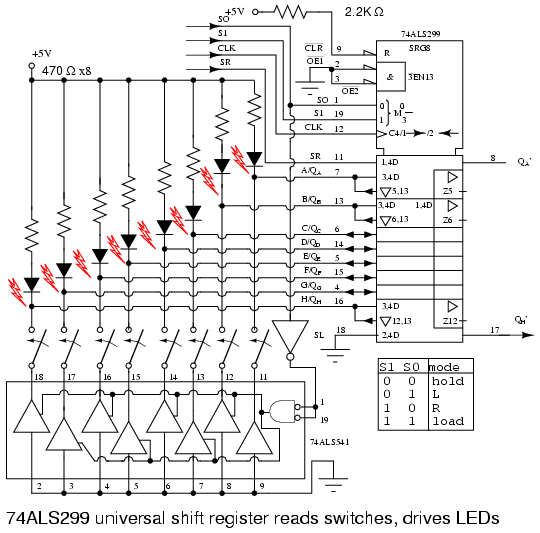
- SN74ALS299 parallel-in/ parallel-out 8-bit universal shift register
We have already looked at the internal details of the SN74LS395A, see above previous figure, 74LS395 parallel-in/ parallel-out shift register with tri-state output. Directly above is the ANSI symbol for the 74LS395.
Why only 4-bits, as indicated by SRG4 above? Having both parallel inputs, and parallel outputs, in addition to control and power pins, does not allow for any more I/O (Input/Output) bits in a 16-pin DIP (Dual Inline Package).
R indicates that the shift register stages are reset by input CLR' (active low- inverting half arrow at input) of the control section at the top of the symbol. OC', when low, (invert arrow again) will enable (EN4) the four tristate output buffers (QA QB QC QD ) in the data section. Load/shift' (LD/SH') at pin (7) corresponds to internals M1 (load) and M2 (shift). Look for prefixes of 1 and 2 in the rest of the symbol to ascertain what is controlled by these.
The negative edge sensitive clock (indicated by the invert arrow at pin-10) C3/2has two functions. First, the 3 of C3/2 affects any input having a prefix of 3, say 2,3D or 1,3D in the data section. This would be parallel load at A, B, C, D attributed to M1 and C3 for 1,3D. Second, 2 of C3/2-right-arrow indicates data clocking wherever 2 appears in a prefix (2,3D at pin-2). Thus we have clocking of data at SER into QAwith mode 2 . The right arrow after C3/2 accounts for shifting at internal shift register stages QA QB QCQD.
The right pointing triangles indicate buffering; the inverted triangle indicates tri-state, controlled by theEN4. Note, all the 4s in the symbol associated with the EN are frequently omitted. Stages QB QC are understood to have the same attributes as QD. QD' cascades to the next package's SER to the right.
The table above, condensed from the data '299 data sheet, summarizes the operation of the 74ALS299 universal shift/ storage register. Follow the '299 link above for full details. The Multiplexer gates R, L,load operate as in the previous "shift left/ right register" figures. The difference is that the mode inputsS1 and S0 select shift left, shift right, and load with mode set to S1 S0 = to 01, 10, and 11respectively as shown in the table, enabling multiplexer gates L, R, and load respectively. See table. A minor difference is the parallel load path from the tri-state outputs. Actually the tri-state buffers are (must be) disabled by S1 S0 = 11 to float the I/O bus for use as inputs. A bus is a collection of similar signals. The inputs are applied to A, B through H (same pins as QA, QB, through QH) and routed to the load gate in the multiplexers, and on the the D inputs of the FFs. Data is parallel load on a clock pulse.
The one new multiplexer gate is the AND gate labeled hold, enabled by S1 S0 = 00. The hold gate enables a path from the Q output of the FF back to the hold gate, to the D input of the same FF. The result is that with mode S1 S0 = 00, the output is continuously re-loaded with each new clock pulse. Thus, data is held. This is summarized in the table.
To read data from outputs QA, QB, through QH, the tri-state buffers must be enabled by OE2', OE1' =00and mode =S1 S0 = 00, 01, or 10. That is, mode is anything except load. See second table.
Right shift data from a package to the left, shifts in on the SR input. Any data shifted out to the right from stage QH cascades to the right via QH'. This output is unaffected by the tri-state buffers. The shift right sequence for S1 S0 = 10 is:
SR > QA > QB > QC > QD > QE > QF > QG > QH (QH')
Left shift data from a package to the right shifts in on the SL input. Any data shifted out to the left from stage QA cascades to the left via QA', also unaffected by the tri-state buffers. The shift left sequence forS1 S0 = 01 is:
(QA') QA < QB < QC < QD < QE < QF < QG < QH (QSL')
Shifting may take place with the tri-state buffers disabled by one of OE2' or OE1' = 1. Though, the register contents outputs will not be accessible. See table.
The "clean" ANSI symbol for the SN74ALS299 parallel-in/ parallel-out 8-bit universal shift register with tri-state output is shown for reference above.
The annotated version of the ANSI symbol is shown to clarify the terminology contained therein. Note that the ANSI mode (S0 S1) is reversed from the order (S1 S0) used in the previous table. That reverses the decimal mode numbers (1 & 2). In any event, we are in complete agreement with the official data sheet, copying this inconsistency.
Practical applications
The Alarm with remote keypad block diagram is repeated below. Previously, we built the keypad reader and the remote display as separate units. Now we will combine both the keypad and display into a single unit using a universal shift register. Though separate in the diagram, the Keypad and Display are both contained within the same remote enclosure.
We will parallel load the keyboard data into the shift register on a single clock pulse, then shift it out to the main alarm box. At the same time , we will shift LED data from the main alarm to the remote shift register to illuminate the LEDs. We will be simultaneously shifting keyboard data out and LED data into the shift register.
Eight LEDs and current limiting resistors are connected to the eight I/O pins of the 74ALS299 universal shift register. The LEDS can only be driven during Mode 3 with S1=0 S0=0. The OE1' and OE2' tristate enables are grounded to permenantly enable the tristate outputs during modes 0, 1, 2. That will cause the LEDS to light (flicker) during shifting. If this were a problem the EN1' and EN2' could be ungrounded and paralleled with S1 and S0 respectively to only enable the tristate buffers and light the LEDS during hold, mode 3. Let's keep it simple for this example.
During parallel loading, S0=1 inverted to a 0, enables the octal tristate buffers to ground the switch wipers. The upper, open, switch contacts are pulled up to logic high by the resister-LED combination at the eight inputs. Any switch closure will short the input low. We parallel load the switch data into the'299 at clock t0 when both S0 and S1 are high. See waveforms below.
Once S0 goes low, eight clocks (t0 tot8) shift switch closure data out of the '299 via the Qh' pin. At the same time, new LED data is shifted in at SR of the 299 by the same eight clocks. The LED data replaces the switch closure data as shifting proceeds.
After the 8th shift clock, t8, S1 goes low to yield hold mode (S1 S0 = 00). The data in the shift register remains the same even if there are more clocks, for example, T9, t10, etc. Where do the waveforms come from? They could be generated by a microprocessor if the clock rate were not over 100 kHz, in which case, it would be inconvenient to generate any clocks after t8. If the clock was in the megahertz range, the clock would run continuously. The clock, S1 and S0 would be generated by digital logic, not shown here.
